← Step Up Amp Research Power Step Wiring Diagram: What's Inside Your Running Boards Amp research power step wiring diagram f150 Haldex Snow Plow Pump Wiring Diagram: Master Your Winter Setup Haldex snow plow pump wiring diagram →
If you are looking for PADS Professional PCB Design | Siemens Software | Cadlog you've visit to the right page. We have 25 Images about PADS Professional PCB Design | Siemens Software | Cadlog like Day1 Basics of PCB Design in PADS | PDF | Printed Circuit Board | Design, PADS Tutorial For PCB Designing | PDF | Printed Circuit Board | Capacitor and also PCB Layout Design by Siemens | PADS Professional | Cadlog. Here it is:
PADS Professional PCB Design | Siemens Software | Cadlog
 www.cadlog.com
PADS Professional PCB Design | Siemens Software | Cadlog
PADs PCB Design Services - Expert Solutions By 911EDA
 www.911eda.com
PADs PCB Design Services - Expert Solutions by 911EDA
PADS Professional PCB Design | Siemens Software | Cadlog
 www.cadlog.com
PADS Professional PCB Design | Siemens Software | Cadlog
The 13 Most Used PCB Layout Design Tools
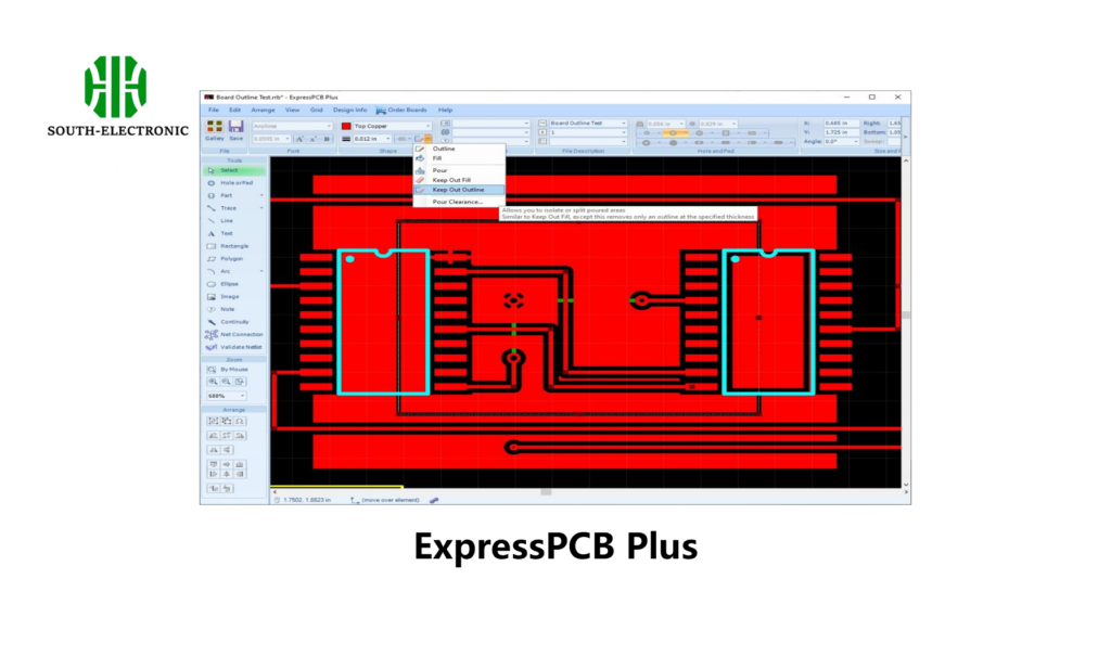 southelectronicpcb.com
The 13 Most Used PCB Layout Design Tools
PADS Layout Tips | PDF | Page Layout | Printed Circuit Board
 www.scribd.com
PADS Layout Tips | PDF | Page Layout | Printed Circuit Board
PCB Layout Design By Siemens | PADS Professional | Cadlog
 www.cadlog.com
PCB Layout Design by Siemens | PADS Professional | Cadlog
PADS Professional - PCB Design Solution | InnoFour
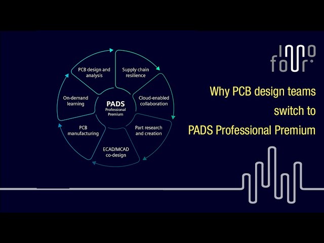 www.innofour.com
PADS Professional - PCB design solution | InnoFour
PADs PCB Design Services - Expert Solutions By 911EDA
 www.911eda.com
PADs PCB Design Services - Expert Solutions by 911EDA
PCB Layout Design By Siemens | PADS Professional | Cadlog
 www.cadlog.com
PCB Layout Design by Siemens | PADS Professional | Cadlog
PADS Standard Layout - Mentor Graphics
 www.pads.com
PADS Standard Layout - Mentor Graphics
PCB Layout Design By Siemens | PADS Professional | Cadlog
 www.cadlog.com
PCB Layout Design by Siemens | PADS Professional | Cadlog
PADS Standard Layout - Mentor Graphics
 www.pads.com
PADS Standard Layout - Mentor Graphics
PCB Design In The Shape And Size Of The Pad Design Standards | Andwin
 www.andwinpcb.com
PCB design in the shape and size of the pad design standards | Andwin ...
Solved Need To Design It In PCB Layout For My Project Using | Chegg.com
 www.chegg.com
Solved Need to design it in PCB layout for my project using | Chegg.com
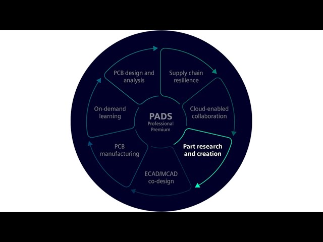
PADS Professional Premium - Complete PCB Design Solution | InnoFour
 www.innofour.com
PADS Professional Premium - Complete PCB design solution | InnoFour
PADS Professional Premium - Complete PCB Design Solution | InnoFour
 www.innofour.com
PADS Professional Premium - Complete PCB design solution | InnoFour
PADS PCB Design Alternatives And Similar Software | AlternativeTo
 alternativeto.net
PADS PCB Design Alternatives and Similar Software | AlternativeTo
PCB Layout Design By Siemens | PADS Professional | Cadlog
 www.cadlog.com
PCB Layout Design by Siemens | PADS Professional | Cadlog
Day1 Basics Of PCB Design In PADS | PDF | Printed Circuit Board | Design
 www.scribd.com
Day1 Basics of PCB Design in PADS | PDF | Printed Circuit Board | Design
PADS PCB Design Software Free Trial
 www.cadlog.com
PADS PCB Design software free trial
Padstack - Reference Pcb Design By PADS Layout - Electrical Engineering
 electronics.stackexchange.com
padstack - Reference pcb design by PADS layout - Electrical Engineering ...
PCB Layout Design By Siemens | PADS Professional | Cadlog
 www.cadlog.com
PCB Layout Design by Siemens | PADS Professional | Cadlog
PADS PCB Design Software – Krishwave
 krishwave.com
PADS PCB Design Software – krishwave
PADS PCB Design Alternatives And Similar Software - AlternativeTo.net
 alternativeto.net
PADS PCB Design Alternatives and Similar Software - AlternativeTo.net
PADS Tutorial For PCB Designing | PDF | Printed Circuit Board | Capacitor
 www.scribd.com
PADS Tutorial For PCB Designing | PDF | Printed Circuit Board | Capacitor
pads pcb design services. Pads pcb design services. Pads professional pcb design