← 1979 Chevy Dual Fuel Tank Wiring Diagram: Install a Dual System Correctly [diagram] wiring diagram for dual fuel tanks Stove Fixes: Solve Your Stove Plate Wiring Diagram Issues for Good Electric stove wiring diagram →
If you are looking for How to Design a PCB Layout you've visit to the right web. We have 25 Pictures about How to Design a PCB Layout like PCB Layout design | FX PCB, A detailed guide to PCB layout design |Qtech Technology Co. Ltd and also Step-by-step cadence PCB design tutorial - RayPCB. Read more:
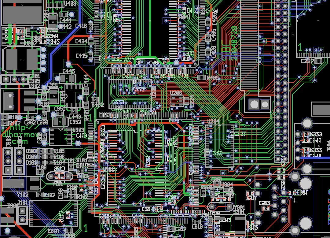
How To Design A PCB Layout
 hilelectronic.com
How to Design a PCB Layout
Altium Pcb Design Tutorial
 wiringfixmount.z13.web.core.windows.net
Altium Pcb Design Tutorial
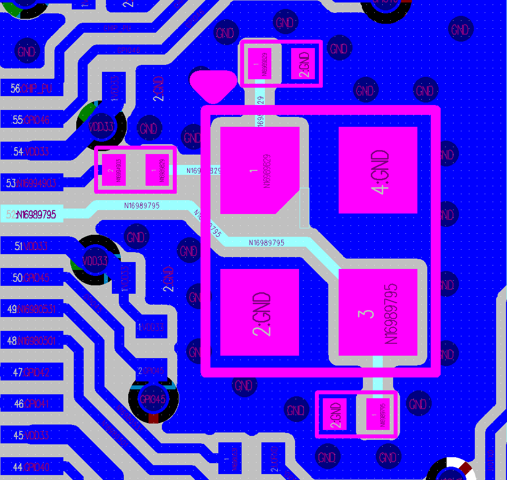
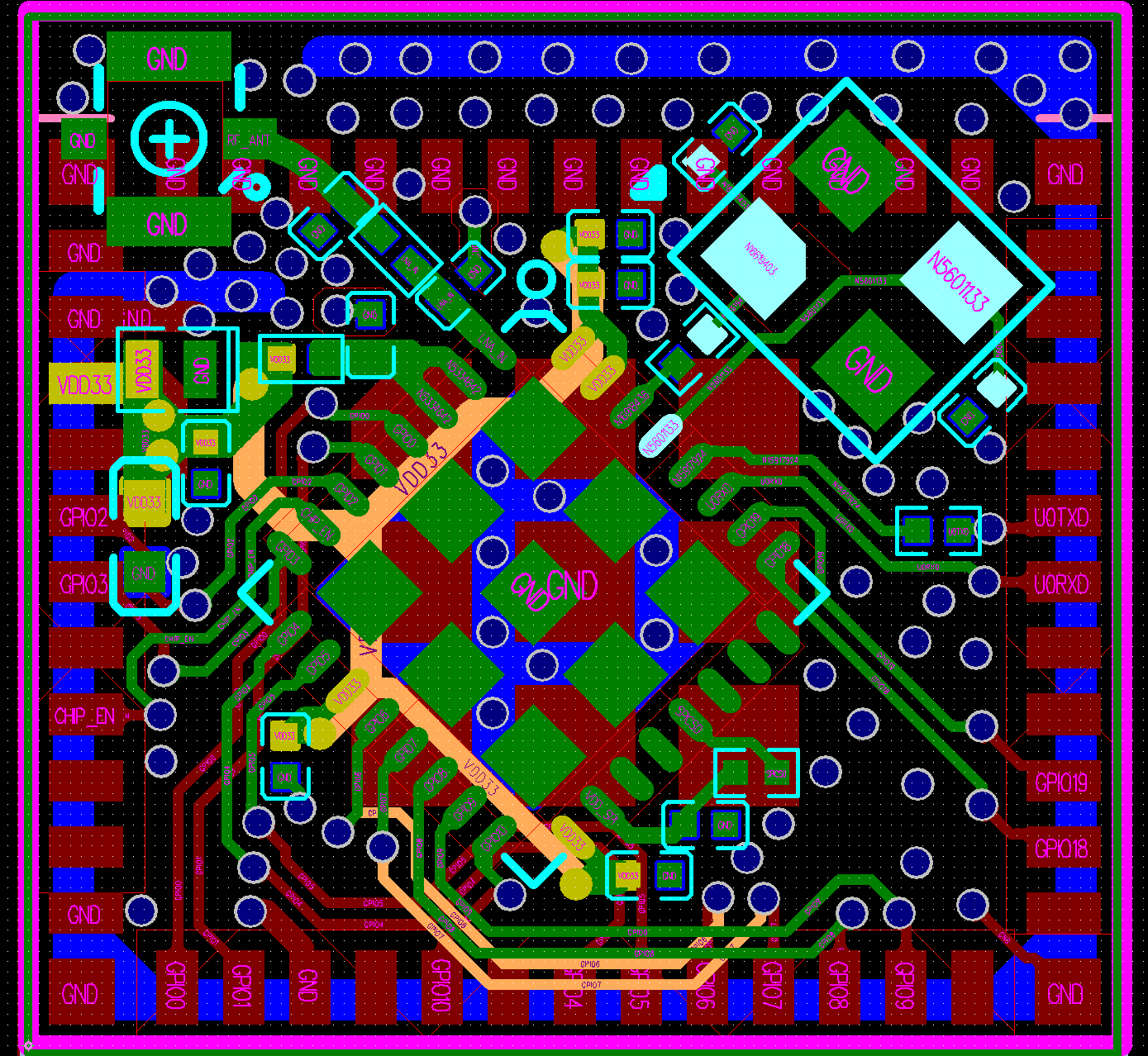
PCB Layout Design - ESP32-C2 - — ESP Hardware Design Guidelines Latest
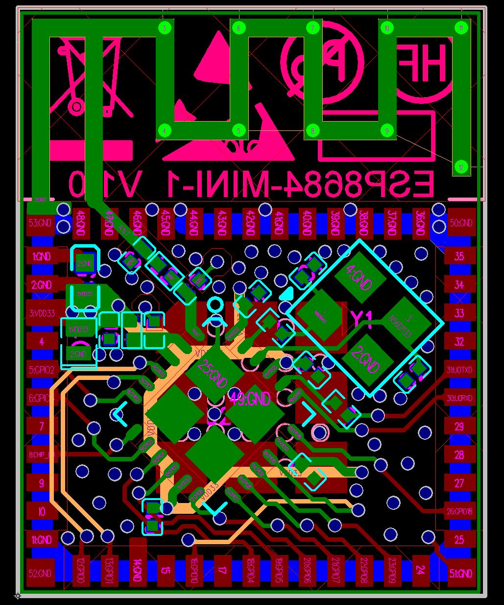 docs.espressif.com
PCB Layout Design - ESP32-C2 - — ESP Hardware Design Guidelines latest ...
Nand Gate Cmos Diptrace Pcb Layout
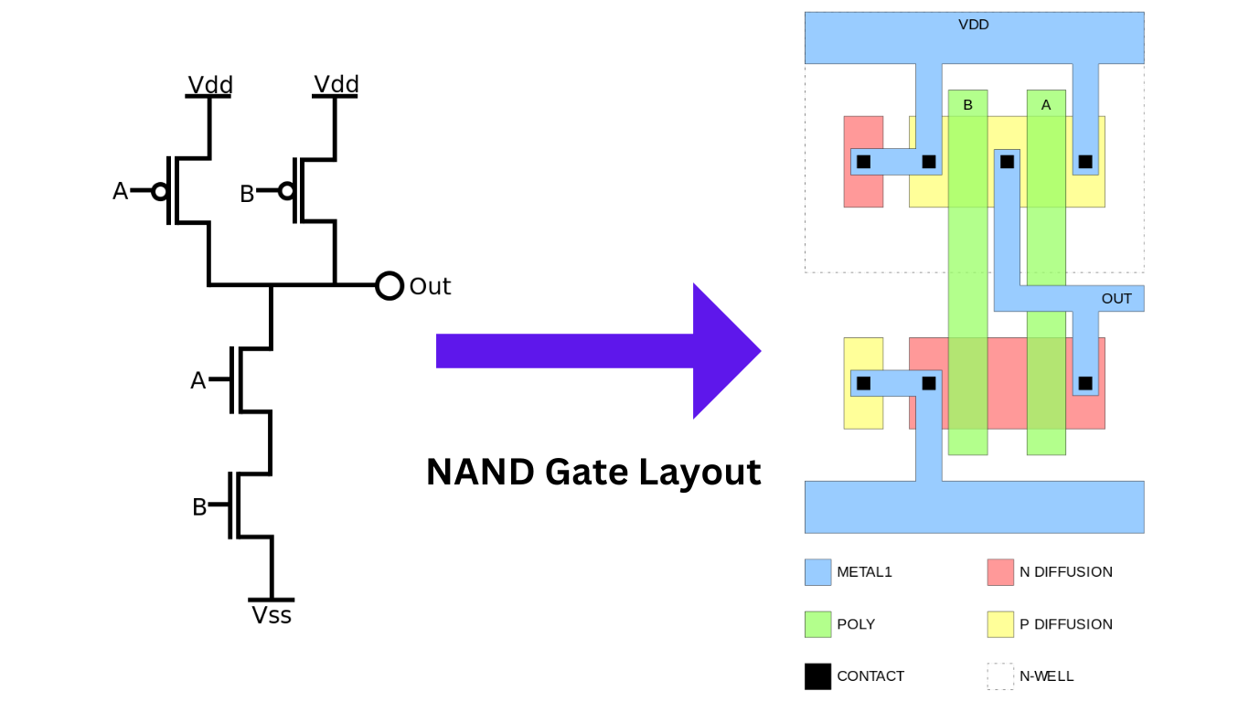 mavink.com
Nand Gate Cmos Diptrace Pcb Layout
A Detailed Guide To PCB Layout Design - IBE Electronics
 www.pcbaaa.com
A detailed guide to PCB layout design - IBE Electronics
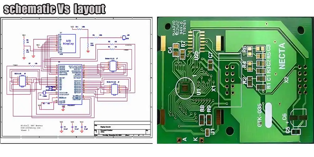
[PDF] Intro To PCB Design: A Beginner’s Guide To Mastering PCB Layout
![[PDF] Intro to PCB Design: A Beginner’s Guide to Mastering PCB Layout](https://www.raypcb.com/wp-content/uploads/2023/02/PCB-Design-Guidelines-For-EMI-EMC.jpg) wiringtoolsreview.blogspot.com
wiringtoolsreview.blogspot.com
[PDF] Intro to PCB Design: A Beginner’s Guide to Mastering PCB Layout ...
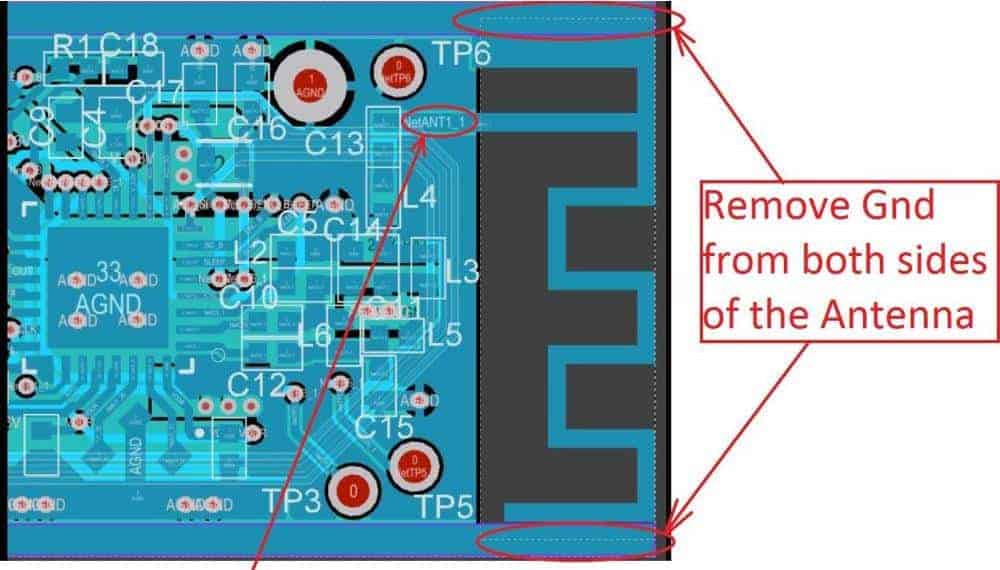
A Guide To The RF PCB Design
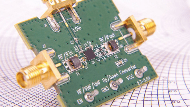 hillmancurtis.com
A Guide to the RF PCB Design
Story Design: Step By Step
 studentpress.org
Story Design: Step by Step
PCB Layout Design - ESP32-S2 - — ESP Hardware Design Guidelines Latest
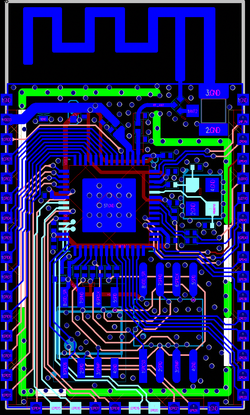 docs.espressif.com
PCB Layout Design - ESP32-S2 - — ESP Hardware Design Guidelines latest ...
Grounding Pcb Crystal Layout Electrical Engineering S - Vrogue.co
 www.vrogue.co
Grounding Pcb Crystal Layout Electrical Engineering S - vrogue.co
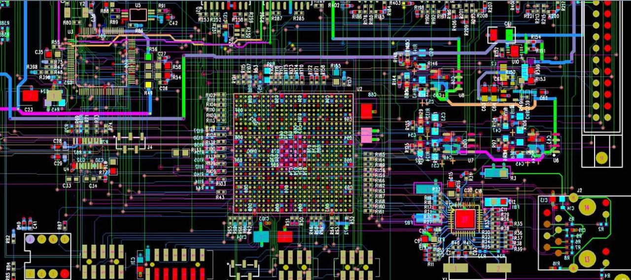
Step-by-step Cadence PCB Design Tutorial - RayPCB
 www.raypcb.com
Step-by-step cadence PCB design tutorial - RayPCB
PCB Layout Design | FX PCB
 sfxpcb.com
PCB Layout design | FX PCB
A Detailed Guide To PCB Layout Design |Qtech Technology Co. Ltd
 qtech-us.com
A detailed guide to PCB layout design |Qtech Technology Co. Ltd
PCB Layout & Design Services In Gandhinagar, India
 www.sbelectronics.co.in
PCB Layout & Design Services In Gandhinagar, India
Four Layer PCB Layout: Design Process And Cost Of Manufacturing
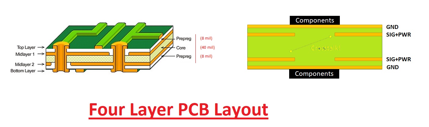 hackaday.io
Four Layer PCB Layout: Design Process and Cost of Manufacturing ...
Complete Guide To PCB Layout Design Steps And Rules – PCB HERO
 www.pcb-hero.com
Complete Guide To PCB Layout Design Steps And Rules – PCB HERO
Circuit Diagram To Pcb Design Software
 guidediagramschoolboys.z21.web.core.windows.net
Circuit Diagram To Pcb Design Software
Mobile App Design: Step-by-step Guide
 www.linkedin.com
Mobile app design: Step-by-step guide
High Speed Pcb Design And Layout, Expert PCB Design Service [ With Step
 www.venture-mfg.com
High Speed Pcb Design and Layout, Expert PCB Design Service [ With Step ...
PCB Layout Design - ESP32-C3 - — ESP Hardware Design Guidelines Latest
 docs.espressif.com
PCB Layout Design - ESP32-C3 - — ESP Hardware Design Guidelines latest ...
Arduino: 2020 Step-by-Step Guide For Absolute Beginners. Everything You
 radiosvat.ru
Arduino: 2020 Step-by-Step Guide for Absolute Beginners. Everything you ...
PCB Layout Design Service: Expert Solutions For Your Circuit Boards
 hillmancurtis.com
PCB Layout Design Service: Expert Solutions for Your Circuit Boards ...
A Detailed Guide To PCB Layout Design - IBE Electronics
 www.pcbaaa.com
A detailed guide to PCB layout design - IBE Electronics
High Speed Pcb Layout Guidelines - Design Talk
 design.udlvirtual.edu.pe
High Speed Pcb Layout Guidelines - Design Talk
Simple PCB Layout Design: Tips And Strategies
 resources.pcb.cadence.com
Simple PCB Layout Design: Tips and Strategies
Circuit diagram to pcb design software. [pdf] intro to pcb design: a beginner’s guide to mastering pcb layout. Four layer pcb layout: design process and cost of manufacturing